최신 브라우저로 업데이트 하십시오.
지금 사용하고 계신 브라우저는 보안 취약점이 발견되었으며,
서비스 이용에 제한을 받을 수 있습니다.

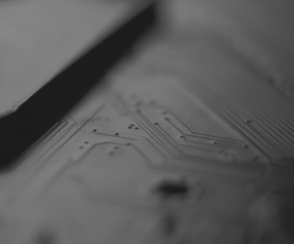
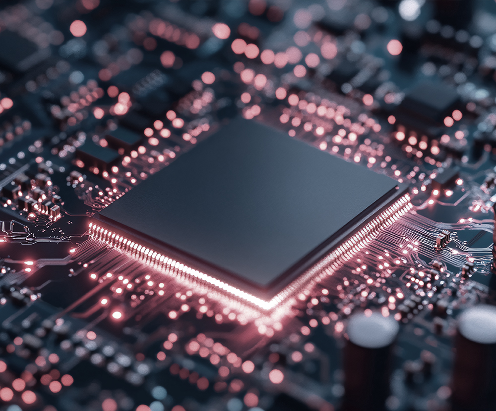

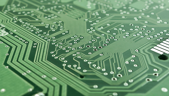
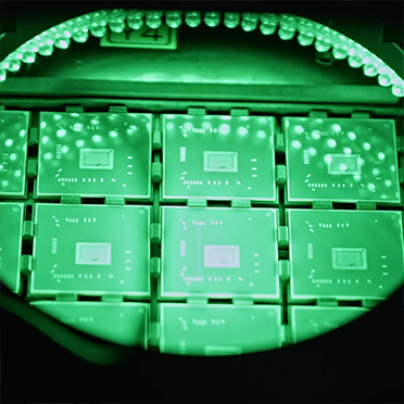
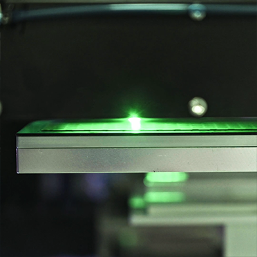
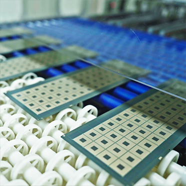
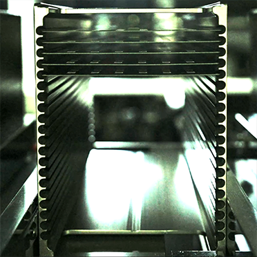
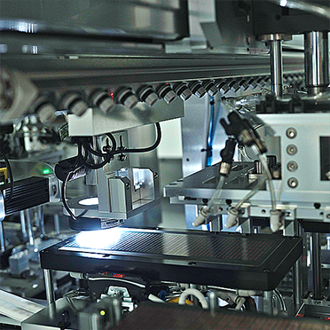
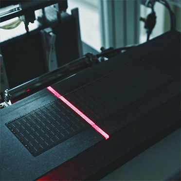
An automated system used to inspect the appearance of a product using a high-resolution camera and lighting system in the final stages of PCB or semiconductor packaging production. It replaces manual visual inspection to ensure quality and defect-free delivery. This equipment is important for inspecting high-density circuits in areas that are difficult to detect with the naked eye, such as Au or OSP-treated pads, and in bonding pads measuring 10μm.
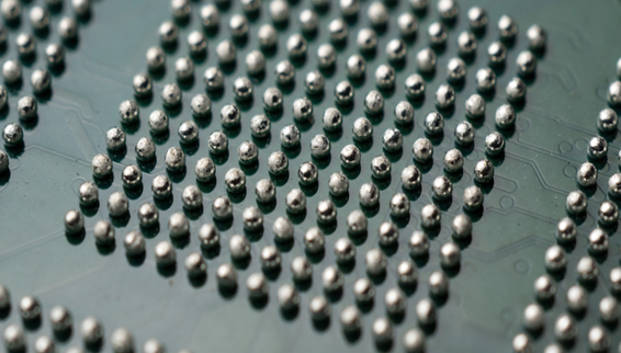
automated system used in the final stage of PCB or semiconductor packaging production to inspect the product’s external appearance and 3D structure with high precision


At DMT, we uncover the smallest details to create the greatest value.